Intel and TSMC's latest advanced nodes compete as key metric shows tight battle for chip supremacy

Amid a push by the Trump administration to have Intel Foundry Services (IFS) bring more contract semiconductor manufacturing to the U.S., early indications are that Intel's 18A process is holding its own against TSMC's first-gen 2nm node known as N2. Both process nodes will go into mass production during the second half of this year with IFS manufacturing a notebook processor codenamed Panther Lake.
Tweets from Dr. Ian Cutress, who is Chief Analyst at More Than Moore (a nice play on the last name of the man who co-founded Intel and came up with Moore's Law), a company that consults with top semiconductor firms, show that Intel's 18A SRAM density of 38.1MB/mm2 is the same figure being reported by TSMC. SRAM density is a measurement showing the amount of SRAM memory that can be found in a given area of a semiconductor chip.
SRAM (Static-Random-Access Memory) is typically used in high-speed applications such as CPU caches (L1, L2, L3). These high-speed layers store data that is often accessed so that the processor doesn't have to wait for slower access to the main DRAM (Dynamic-Random-Access Memory) memory. Higher SRAM density allows for larger caches which, of course, tends to improve performance.
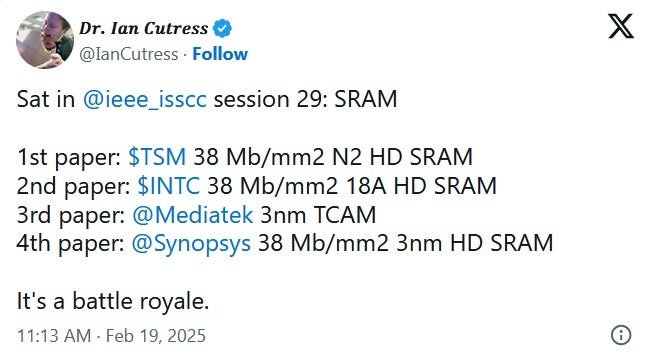
Intel and TSMC battle over process leadership. | Image credit-X
TSMC's 2nm process kicks off its use of Gate-all-around transistors (GAA) replacing FinFET. Using horizontal nanosheets stacked vertically, these transistors allow the gate to come into contact with the channel on all four sides reducing current leaks and resulting in faster speeds and higher drive current. TSMC's first-gen 2nm node delivered a 12% increase in SRAM density while high-performance SRAM density rose 18%.
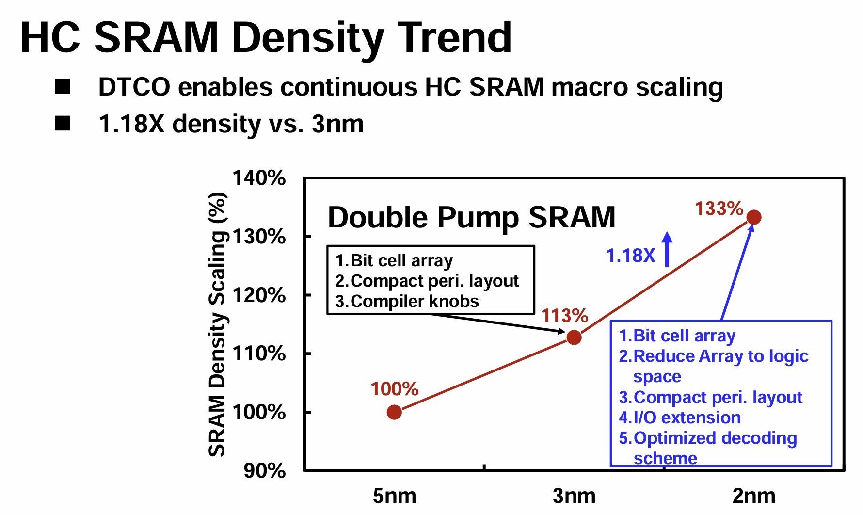
TSMC's HD SRAM density is up 18%. | Image credit-"X
Intel's Power Via feature helps it improve SRAM density for its 18A process. Also known as BSPDN (Backside Power Delivery), this technique moves power delivery networks (PDN) from the top of the silicon wafer to the bottom. The old technique took up too much space limiting the SRAM density.
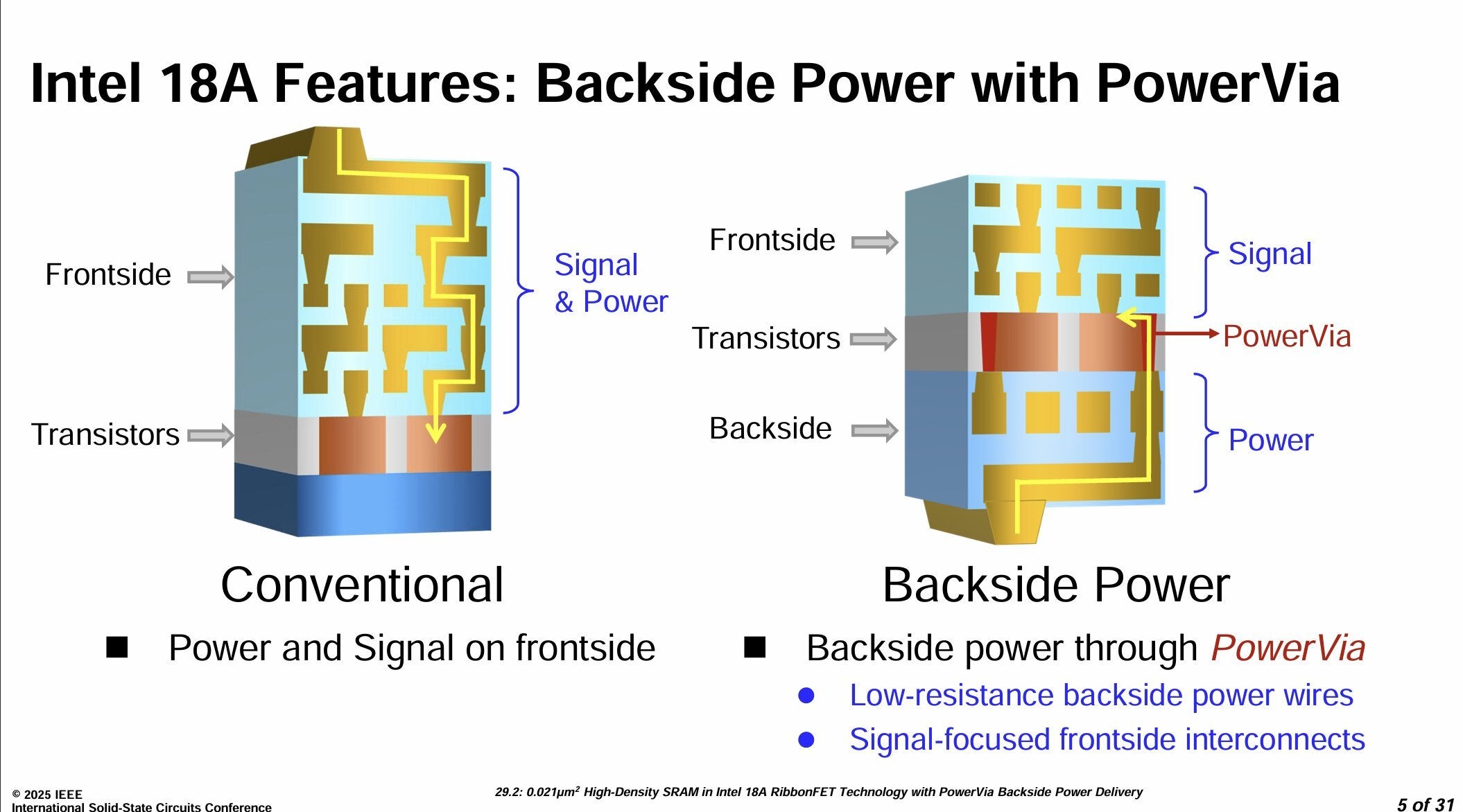
Intel's backside power delivery known as Power Via helped its SRAM density at 18A. | Image credit-X
It's important to note that the density figures can change depending on the structure of individual SRAM memory cells. The real fireworks will come once we see the results of the 18A and N2 process nodes in the form of actual components used to power new devices.
Intel has signed up Amazon's AWS which is interested in using the 18A node to produce chips for internal use with its data centers and AI technology. Microsoft and Broadcom are both also interested in creating designs based on 18A. Companies showing interest in TSMC's N2 include the same old gang such as Apple, MediaTek, Nvidia, Qualcomm, and ironically, Intel.


Things that are NOT allowed: