TSMC tossing silicon wafers in garbage cans near fabs not considered "chip binning"

After a chip is manufactured, testing is done to measure its clock speed, power consumption, the number of working cores, and more. After testing, the chips as classified by how they perform. Top-performing components are placed in the top bins and are sold as high-end silicon. Other chips that don't make the grade are placed in lower bins and command reduced prices. A chip with one defective core could be sold as having seven cores instead of eight, for example.
This practice is known as "Chip Binning" and while not really part of this practice, a Reddit subscriber happened to find a silicon wafer in the ultimate bin-a garbage can. The foundation of chip manufacturing, the wafer was discovered in the dumpster near TSMC's Fab 16 located in Nanjing, China. This fab does not produce some of the high-profile advanced process node chips you've heard about such as 4nm, 3nm, and the 2nm node that TSMC will start mass producing during the second half of this year. The factory in Nanjing turns out chips using 12nm and other integrated circuits manufactured using mature nodes like 16nm and 28nm.
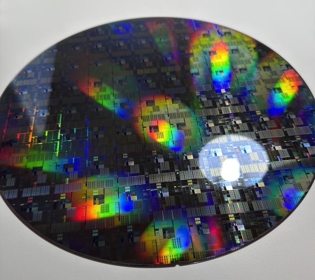
Test silicon wafer found by a Redditor in a dumpster near TSMC's Fab 16. | Image credit-Reddit subscriber AVX512-VNNI
The silicon wafer found by Reddit subscriber AVX512-VNNI cannot be diced into GPU chips for AI companies like OpenAI (which just announced that it is all out of GPU chips) even though each wafer can contain hundreds of chip dies. That's because the particular wafer found by the Redditor is a test wafer equipped with dummy circuitry. The test wafer is created to test the lithography machines used to etch circuitry on the wafers that are eventually sliced and diced into chips.
Some of the other Reddit subscribers had good ideas about what to do with the wafer with some suggesting that it be placed inside a picture frame and put on a wall where it could be displayed like a work of art. Considering what these wafers are for, what they do, and the amazing devices powered by the chips cut from them, no one can deny how valuable such art would be.
Most of the responses were jokes with one calling for the use of diamond-tipped pizza slicers to dice the wafer. But with the space between chips only .5mm, you would need to be an expert in cutting pizza slices in order to dice a silicon wafer should you find one of your very own.


Things that are NOT allowed: